- AUTOCUTS
- CCD camera
- CryoMatrix® holey Grid
- Magnetic Field Cancelling System
- Vibration Isolation System
- HATA-Holder System
- PIE plasma cleaners
- Nexperion SentineL
- WET-SEM
- Temassist-Towards Automatic TEM solutions
- FEG and LaB6 filament
- Compressors
- Chiller
- Vacuum System
- High-vacuum Optical Platform for cryo-CLEM
- Quick Freeze Substitution Equipment
- Agar Auto Sputter Coater
- Coating instrument
- Cryo-FIB sample preparation
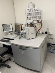
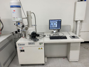
- Nanometer Pattern Generation System
Product Details
NPGS provides a powerful, versatile, and easy to use system for doing advanced beam or ion beam lithography using a commercial SEM, STEM, HIM, FIB, or dual beam (SEM/FIB) microscope. The success of NPGS is demonstrated by the strong recommendations from current users which have resulted in over 490 installations around the world.
NPGS is a tool which can be used in a wide variety of applications. The basic lithography process allows patterns to be defined on aflatsurface.Thesubsequentprocessing,suchas metal I evaporation or etching, will determine the final structure. NPGS is unique in that it provides a very flexible system which is ideally suited to the wide range of activities in basic research and R&D activities. Examples of some of the structures made with NPGS include: single electron devices, quantum chaos devices, quantum dots, tunnel junctions, one and two-dimensional metal wires/films, linear/circular gratings, surface acoustic wave (SAW) devices,split gate devices, as well as"larger'structures such as micromechanical devices, waveguides, and bonding pads. SinceNPGS is so versatile, it is well suited for use in almost any application that can be done with SEM based e-beam lithography.
NPGS can also be used for lithography with a Focused lon Beam (FlB) or Helium lon Microscope (HIM). In fact, a single NPGS installation can be configured with a dual mode to control either the electron beam or the ion beam on dual FIB/SEM systems.
For more detailes, please contact us.
Product appearance